In the semiconductor manufacturing field, as the process shrinks to 7nm and below, traditional materials have reached their physical limits. Due to the increasingly harsh plasma environment and the tightening of thermal budget, it has shifted from being an edge component to a key core component that determines the yield and performance of the wafers.
1. The Material Science Behind the Wafer
The semiconductor front-end process is a battleground of extreme chemistry and physics. Three materials have emerged as the "gold standard":
-
High-Purity Alumina (Alumina Ceramics, 99.8%+): Known for its exceptional dielectric strength and plasma resistance. It is the primary choice for gas distribution plates (showerheads) and chamber liners where preventing metallic contamination is non-negotiable.
-
Aluminum Nitride (AlN Ceramic): With a thermal conductivity exceeding $180\ W/m\cdot K$ and a Coefficient of Thermal Expansion (CTE) closely matched to Silicon, AlN is indispensable for electrostatic chucks (ESC) and rapid thermal processing (RTP) components.
Silicon Carbide (Silicon Carbide ceramics): Specifically CVD-coated SiC, which offers extreme hardness and resistance to erosion in fluorine-based etch chemistries.
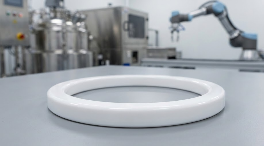
High-precision alumina ceramic ring in a semiconductor cleanroom environment
2. The Engineering Challenge: Precision Machining at the Micron Level
Having the right material is only the starting point. The true value lies in the [Precision Machining] fidelity. For semiconductor applications, we focus on three critical pillars:
- Surface integrity: We can achieve a surface roughness of $Ra < 0.1\ \mu m$ to reduce "particle traps" - those microscopic pits that may hide contaminants and eventually lead to the scrapping of the wafers.
- Geometric complexity: With advanced technology, we are capable of machining complex cooling channels and micro-pore arrays (with diameters typically less than 0.5 mm), while ensuring no chipping at the edges.
- Purity control: The ultrasonic cleaning process after processing ensures that the parts do not contain any residual cutting oil or metallic trace elements.
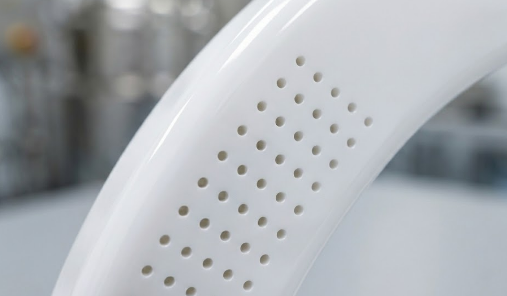
Macro shot of precision micro-hole drilling on a technical ceramic component
3. Why Partner with a Ceramic Specialist?As chip architectures evolve toward 3D-NAND and complex heterogenous integration, the "cost of failure" for a single ceramic component can reach hundreds of thousands of dollars in lost wafer lots. Sourcing from a partner who understands contamination control and thermal management is no longer optional—it is a strategic necessity.
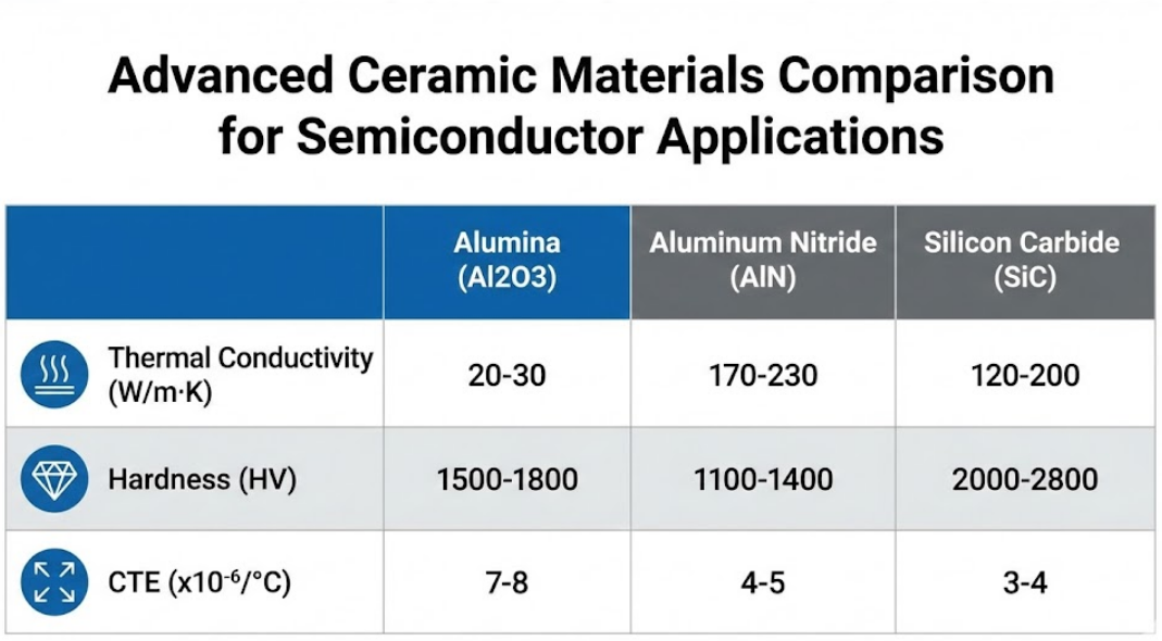
Comparison chart of thermal conductivity, hardness, and CTE for Alumina, Aluminum Nitride, and Silicon Carbide
Ready to optimize your semiconductor process? [Contact UsGet a Quote]]


